News, Updates and Other Minutiae
September 2023 Long time between drinks, but not much happening on the tech front at the moment. Added another couple of rants to the rant page.
January 2023 Updated the AD9833 VFO code to use a 12F1840.
December 2022 Added rant about todays useless (internet) search engines.
November 2022 NEW Project An AD9833 Based Simple VFO. FT101ZD VFO project updated.
October 2022 A replacement internal DDS VFO for FT101Z/ZD rigs. Because the worlds postage system has gone totally bonkers and it is not possible to send a small pcb anywhere except at extreme cost, I am slowly making available the option to purchase pcb's from Pcbway. First up is the Simple DDS VFO 2017 project pcb. Others will be added over time. Noise Canceller kits available again- see Noise Canceller page.
Privacy Policy uploaded. GPDR and all that stuff In accordance with various bits of legislation around the world, either currently in force, about to come into force or proposed, you will now find that annoying "We use cookies" notice at the top of this website. The full Privacy Policy is available at the Privacy Policy link in the footer at the bottom of the page. (If you don't know what GPDR is, Google it. Real scary shit for ANYBODY with a web presence.)
FT101ZD DDS VFO
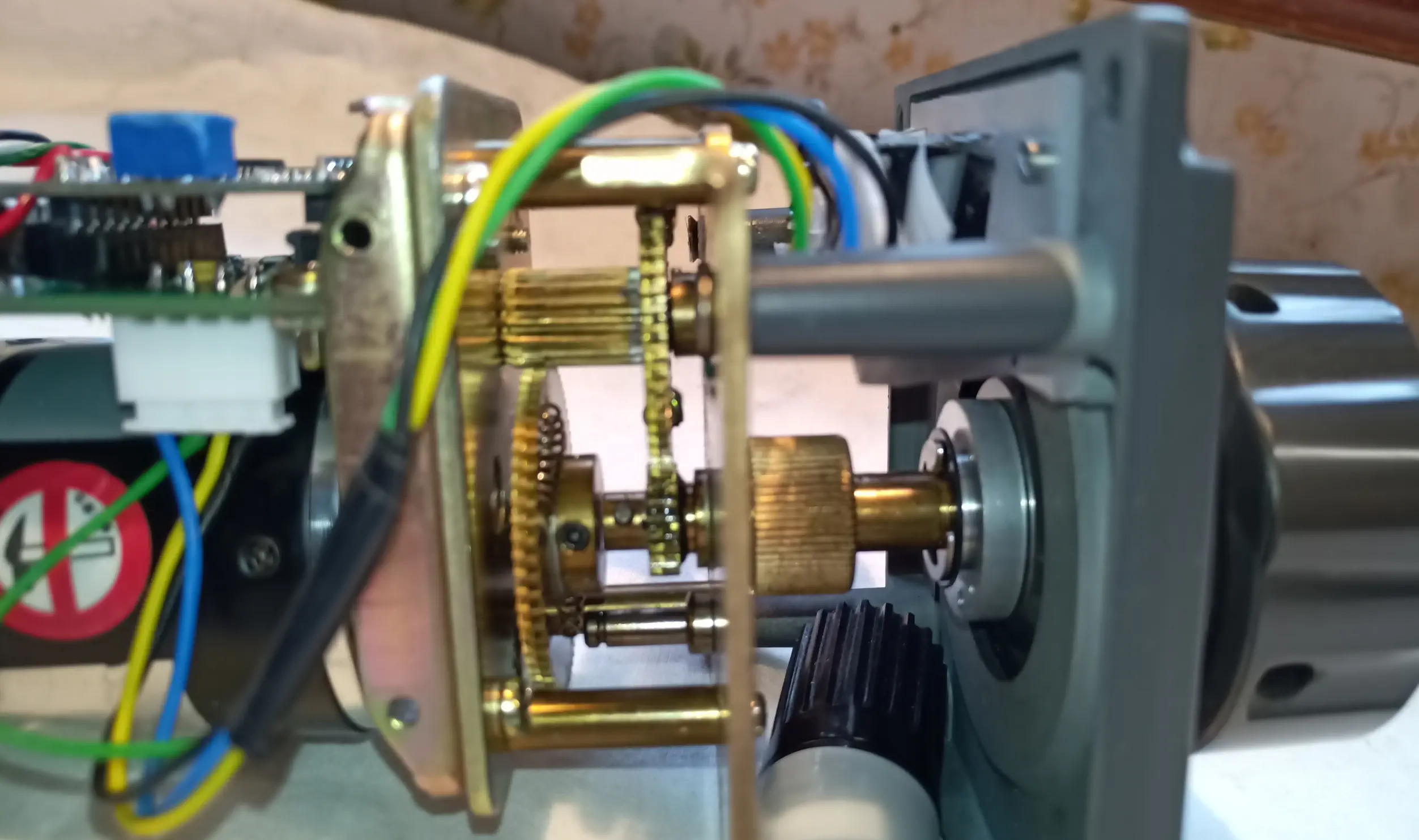
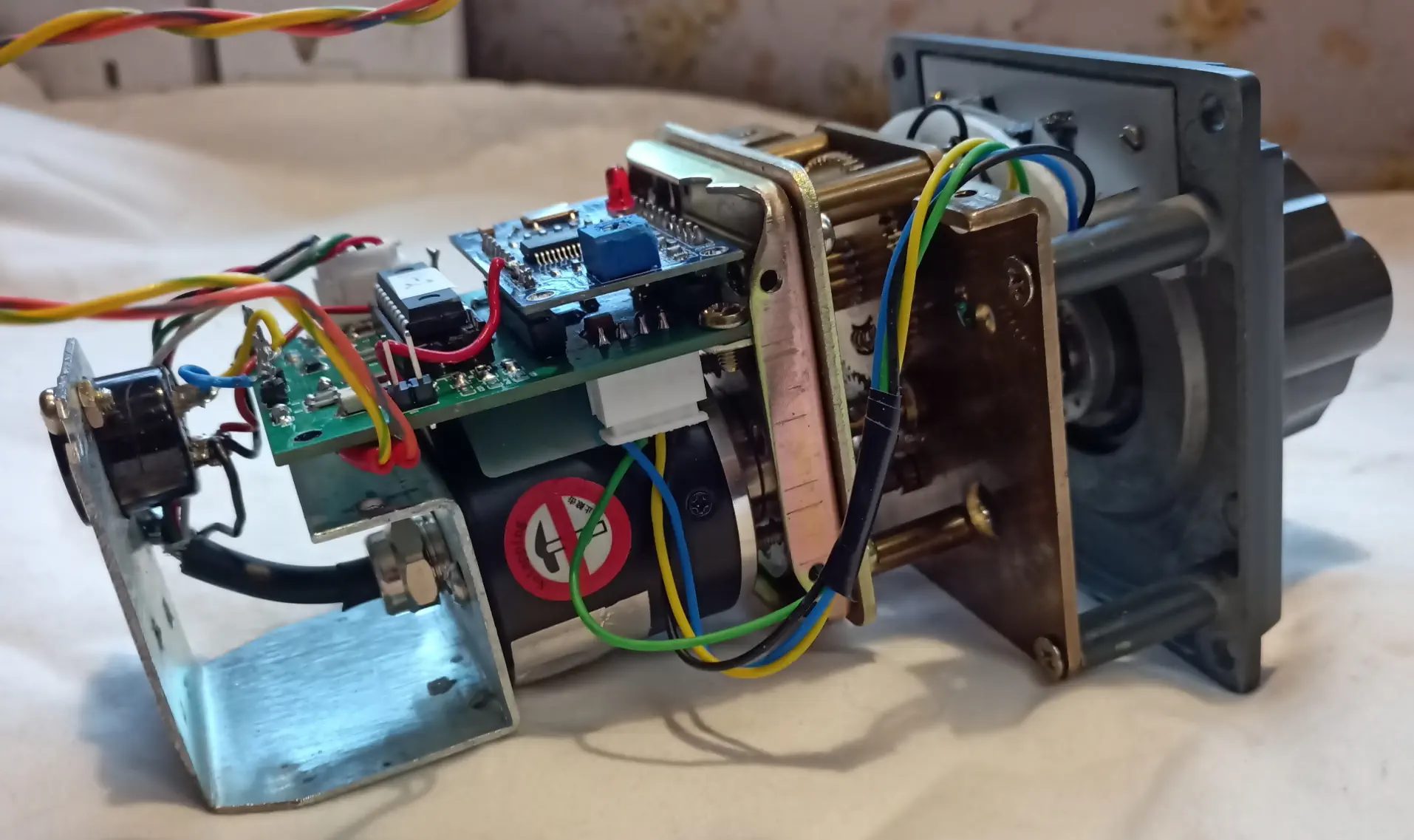
An AD9850 DDS VFO for the FT101ZD. Schematic updated 8 Nov 2022 This project is designed as a replacement for the original internal VFO of the Yaesu FT101Z/ZD rigs. It will probably fit a number of other rigs with some modification. While the AD9850 module might now be a bit dated (and expensive compared to what they were originally), the co-designer of this project, Rod G0IYQ, had them on hand. It uses the original gearing to drive a 360 PPR (Pulses Per Revolution) optical encoder and is compatible with the original Clarifier/RIT control. There is some mechanical work required to interface the encoder to the gearing, a mounting bracket for the electronics (using mostly SMD components) and an addition to the power supply so this is not a beginners project. The encoder was also modified to have the connecting cable exit the rear of it's housing instead of out the side. However you arrange the mechanical aspect of this project, ensure that you can refit the original VFO sheilding can.
(Click pictures for larger view. Click again to close.)
Power supply addition
The addition to the power supply of the FT101Z/ZD is to add another 6V regulator to power the DDS VFO. You will need a 7806 or equivalent voltage regulator to mount on the same panel as Q3, the 8v regulator. Mount the 7806 directly to the panel without an insulator (don't forget to use some heatsink compound). The input of the 7806 is connected to the 12v point on the RECT A UNIT. Also carefully connect 0.1μF caps between the input and output pins to ground of the 7806 plus a 1000μF 35V electrolytic capacitor from the input and output pins to ground. The output of the new 6V regulator is connected to pin 3 of the VFO connector P15/J801 - first carefully remove the existing wire, insulate the end and secure it out of the way and then fit the new connection from the 7806. Ensure that none of the 7806 pins or capacitor connections can short to the chassis (except for the ends connected to ground of course).
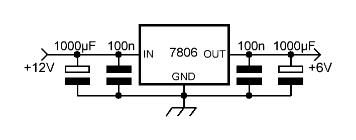
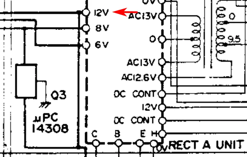
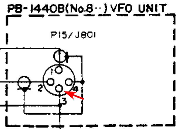
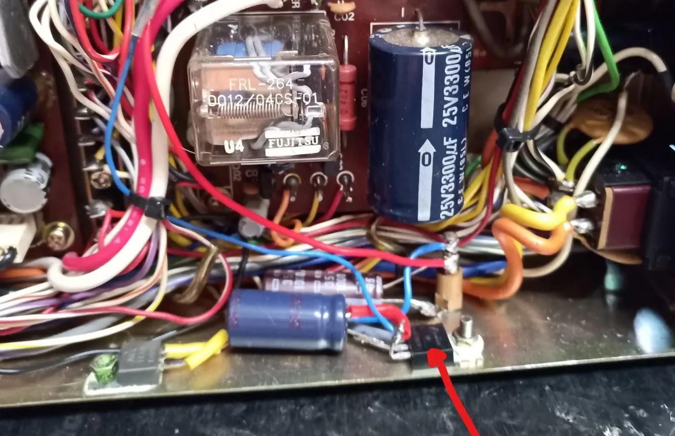
(Click picture for larger view. Click again to close. New 7806 arrowed.)
Step LEDs
In Rod's rig, he has removed the original frequency dial and made a panel with the step size LED's on.
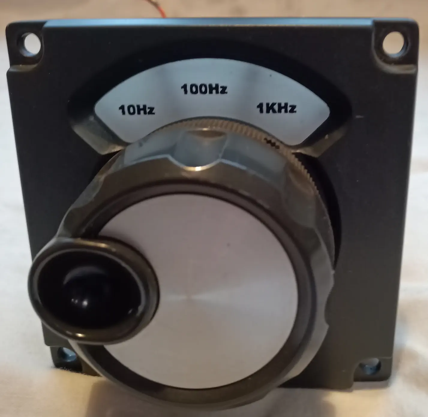
For the step size switch, Rod replaced the "Dim" pot with another that incorporates a push switch (he found it in the junk box), so now it does the dual function of dimming the display lamps and selecting the step size. The pot he used has a value of 10k rather than the original value of 5k which restricts the adjustment range somewhat, but he only ever sets it to full brilliance, so that is of no consequence for him. For those that want to follow that route, (as at October 2022) Mouser in the US has a pot - part # PRS11R-415F-S103B1 - you can use. That is the only one we have been able to find that is available (again a 10k pot) with a push switch. An alternative, if you don't use the Dim control other than at a preset brilliance, is to replace the pot with two resistors (measured from the original pot) and fit a monetary push switch in it's place. This way, you don't have to deface the front panel by drilling another hole somewhere to fit the switch. While not tried as yet to see if it works, to regain the full brilliance range, try connecting a 10k resistor from the 10k pots wiper to ground if you go down that path. I have played with some variable rate tuning code to eliminate the need for the switch, but so far it doesn't have a very "comfortable" feel to it, that is an ongoing quest.
The Electronics
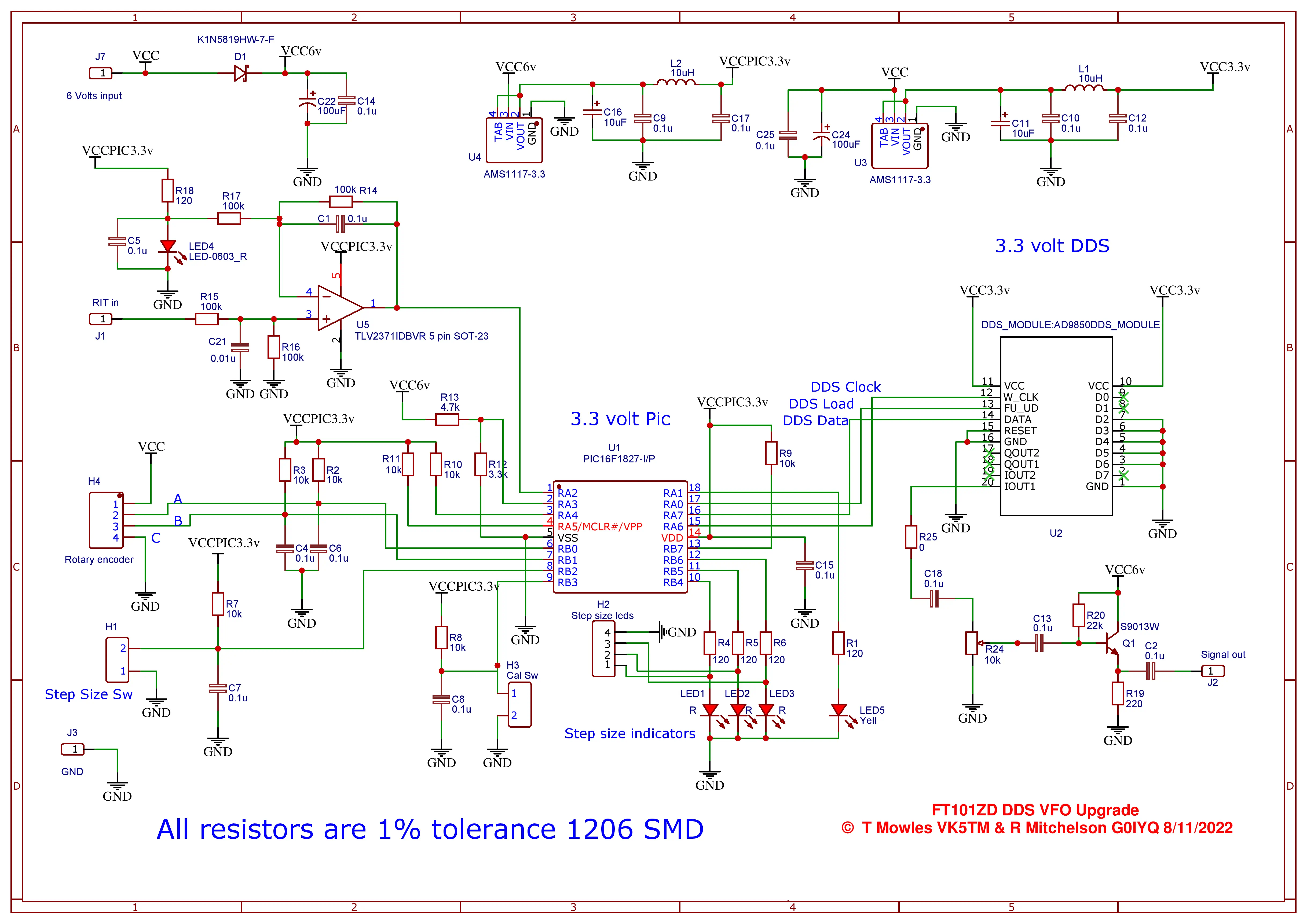
A query re the level of drive required by the FT101Z/ZD led to Rod making some measurements. Original factory VFO outputs a 700mV signal, the DDS VFO has now had the buffer amp values adjusted and the output is slightly higher at 750mV (the previous published values led to a slightly lower output level). The basis of this project are the other DDS projects elsewhere on this site with some significant changes and additions. Firstly, a run down of the functions available: 1/ AD9850 signal generation - frequency range 4.9MHz - 5.6MHz in line with the original VFO specs. 2/ 10Hz, 1kHz & 10kHz switch selectable step sizes with LED indication. 3/ Clarifier/RIT that uses the original front panel control and works on both Rx and Tx as per the original. 4/ Save of VFO frequency & step size on power down - in the original DDS project, this was done 2 seconds or so after the encoder stopped moving after every frequency change. 5/ Processor changed to 16F1827.
(Download a PDF version in the Downloads section.)
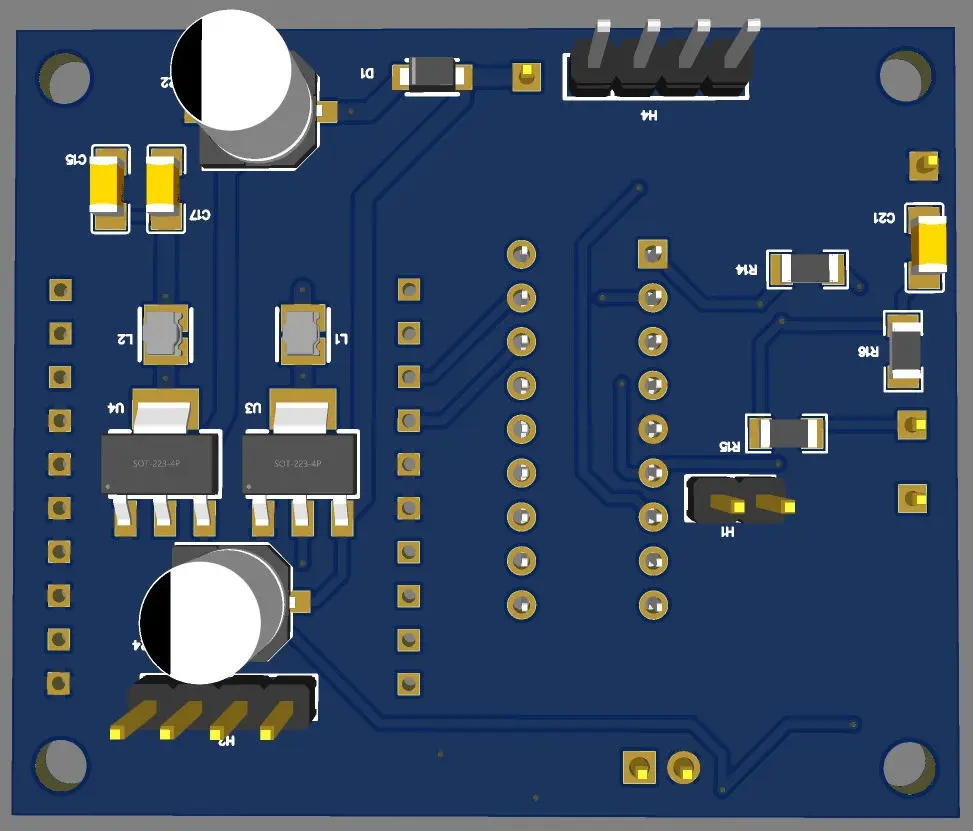
Running through the schematic, an explanantion of the various circuit blocks: 1/ The power supply. It may seem a bit extreme to have all the various bits that there are, but there is a reason (or two). Firstly, the last thing you want is digital noise getting back in to the rig and secondly some of it is to enable the power down save function. The whole lot runs off the 6V supply from the previously mentioned 7806 addition, which is split between two low drop 3.3V regulators. 6V is applied directly to the optical encoder as well as one of the low drop regulators to supply the DDS unit (Note that all the AD9850 modules suppled now seem to be of the 3.3V variety). The second low drop regulator that powers the PIC is supplied via a Schottky diode which is also connected to a voltage divider that feeds in to one input of the PIC. On power down, the Schottky diode prevents the 100μF capacitor discharging back in to the 6v supply line and the falling voltage is detected by the PIC via the voltage divider. An internal comparator in the PIC references the falling voltage with an internal reference voltage and triggers the power down save routine in software when the falling voltage from the divider gets below the reference voltage. 2/ The Op-Amp circuit. On the FT101Z/ZD rigs (and possibly others), the Clarifier provides a control voltage to the original VFO that varies between ~2V and 5V which offsets the frequency of the VFO by a small adjustable amount (nominally ± 0-2.5kHz). Because the PIC does not have 5V tolerant inputs when running with a 3.3V supply, this Clarifier voltage can not be connected directly to the PIC so we use what is basically a differential amp circuit. This circuit translates the ~2 - 5V at it's input to an output range of ~0 - 3V, which is safe to connect to the PIC. This ~0 - 3V is measured by the ADC (Analogue to Digital Converter) and the software uses the reading to adjust the frequency of the DDS by the above mentioned offset. 3/ Rest of the circuit. The rest of the circuit is in what we can call the "nothing special" category (other than the PIC being the brains of this whole project) and consists of various inputs and outputs to/from the PIC and the AD9850 DDS module. LEDs are used to indicate the selected step size (10Hz, 1kHz or 10kHz) and to indicate when the Clarifier is in it's "zero" or no offset position (more about that later). A small buffer amp prevents the FT101Z/ZD's circuit loading the output of the DDS module. Note that capacitors C4 and C6 on the schematic are not used, they are a relic from the mechanical encoder days and provision has been made for them on a "just in case" basis. 4/ Software. Not strictly "in the schematic" but I think a convenient place to at least mention it. The software is modified from the various DDS files on this site with quite a lot of changes/additions - note that it is only suitable for non-detented optical encoders (the cheapy mechanical ones won't work here) and is only for the AD9850. I'm not going to do a blow by blow run through of the code - there is a lot of it - but the ASM file is fairly well commented so you should be able to work out what is going on. The basic flow of the program is, on power up, do all the initial setup and check inputs and outputs. Set the various outputs and DDS frequency to the last saved values plus any offset if the Clarifier control is not zeroed. After all that is done, the software then enters a loop that checks the Step Size switch input, Clarifier input and Encoder input for any changes. If a change is detected, the software branches out and performs the functions associated with whatever changed. After completing the requred function, the software returns to polling the inputs. Also, the software continuously monitors for a power down condition and will branch off into the frequency and step size save routine if a power down condition occurs. The software does not return from this function until the power has been turned off and back on to prevent any corruption of the data, if the power down condition was caused by a glitch on the supply rails, rather than the rig actually being turned off. 5/ A Note re the Clarifier control and zero LED. At this point, only one rig has been modified and it was noticed that at the extreme end settings of the Clarifier control, the offset would occasionally flicker about. We think it is to do with the op-amp circuit but that is still to be investigated properly. In the meantime a very simple cure if you strike the same problem is to fit a 10k resistor across the Clarifier pot. It does reduce the offset slightly to ~±2kHz, so try experimenting with the value of the resistor if you feel the need to have the full ±2.5kHz range. Now for the Zero LED. This was added mainly as an aid to setting the Clarifier pot to it's center or zero offset position at 12 o'clock on the front panel. The manual for these rigs contains a procedure for adusting this so that the Rx and Tx zero setting is at the same point. Now, instead of having to check the frequency, you can set the adjustment while watching for the zero LED to turn on. Note that there is a small dead band (equal to zero offset) around the center point of the pot. Also when making the adjustment, move the control slowly or you might miss the LED turning on.
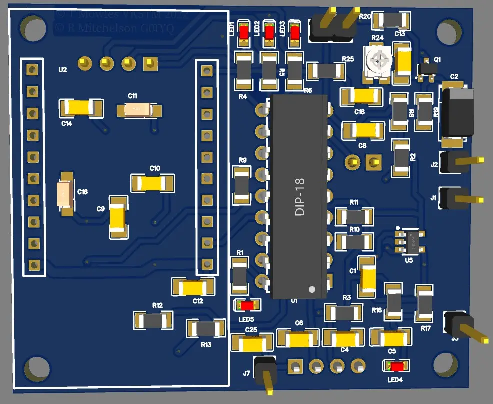
PCB
The pcb was designed by Rod using EasyEda from JLCPCB. It is fairly compact as it is designed to fit within the original sheilded area and the smd components are 1206 sized where possible. Although not shown below, it is advisable to fit a socket for the PIC (shown in the pictures above). As is standard policy on this website, the pcb files will not be made available (so please don't ask), but arrangements are being made for interested builders to get pcb's. I will put a note at the top of this page as soon as it has been organised. At this stage, it is not envisaged this project will be supplied as a kit.
Calibration
As with the other DDS projects, there is an inbuilt calibration routine to account for the xtal oscillator on the AD9850 module being off frequency (most of them are). Once you have built the unit, it really should be calibrated before you fit it in to the rig. Calibration requires the use of an accurate frequency counter with 1Hz resolution and is used to adjust the "OSC" values in software to correct for off frequency Xtals on the DDS modules. Connect the frequency counter to the output of the unit (J2) and short the header pins marked "H3" on the pcb. The short must not be removed until calibration is complete. With the pads shorted, apply power. The frequency counter should show a frequency somewhere in the vicinity of the calibration value - 5.250MHz - in this software. Go away and have a cup of coffee, maybe a biscuit or 2 or what ever your choice. Once you have left the unit to run for a minimum of fifteen minutes, then continue. Or in other words, give it time to warm up before doing any adjustments (and keep it out of any drafts). Turn the encoder in which ever direction is required to change the frequency so that the frequency counter reads - as exactly as possible - 5.250MHz. Note that the oscillator calibration steps are very small, so you may have to turn the encoder a fair number of turns to reach the calibration frequency. Without turning the encoder further, remove the short from H3 and then turn the encoder again (direction does not matter). This will save the new computed "OSC" values into EEPROM and the unit will now be functional. At this point, you can remove power and fit it into the rig. Note that the calibration routine can be done any time, it is not locked out if it has been done previously and there is no need for a 'reset' function as with some of my other DDS projects.
Ongoing work
As with most of my projects, there is the possibility of upgrades or other changes, they will be posted here when/if anything changes. Having said that, there are two or three things being looked at, one is the variable rate tuning option and the other is a different frequency generating device, hopefully smaller and cheaper than the AD9850 modules (not the Si5351). The third thing is in relation to the Clarifier/RIT input to make this project available for a wider range of rigs - this is just a thought bubble at the moment.
Downloads
These files are provided free for personal use ONLY. I retain copyright on all works published on this website unless otherwise noted. These files, or any derivative of them, may NOT be used in any commercial or profit making enterprise of any kind without the express WRITTEN permission of the copyright holder.
(Right click and 'Save as..' or what ever is required by your browser) Schematic_FT101Z DDS VFO V0.2.pdf Schematic in PDF format. Updated 8 Nov 2022 BBOM_FT101Z DDS VFO V0.2.csv Parts list in CSV format. Updated 8 Nov 2022 FT101Z_VFO_V1-2_VK5TM.asm FT101Z_VFO_V1-2_VK5TM.HEX
