News, Updates and Other Minutiae
August 2025 UR5WHK has created another version of the AD9833 project with a 128 X 32 OLED display. You can find it under the Gallery menu - it is on the same page as the MAX7219 version.
July 2025 UR5WHK has created an updated version of the AD9833 project which now includes a MAX7219 based LED display. Code updated 10 July 2025. Code updated again 15 July 2025. You can find it under the Gallery menu.
March 2025 In something of a "Seniors Moment", I forgot to update the homebrew menu and this section relating to a project I did late 2024. That project is an update of one from the RSGB Radcom magazine of Sept 1999 - 'Turn Your Dip Meter into a Signal Generator'. Presented here as 'Grid Dip Meter (GDO) Add on' under the Homebrew menu.
November 2024 Phillipe F6ETI has done some serious testing on the Noise Canceller and shown it works up to 72MHz and is usable with some loss at 145MHz. Links to his website with photo's, video's and description of the testing on the Noise Canceller page.
Privacy Policy uploaded. GPDR and all that stuff In accordance with various bits of legislation around the world, either currently in force, about to come into force or proposed, you will now find that annoying "We use cookies" notice at the top of this website. The full Privacy Policy is available at the Privacy Policy link in the footer at the bottom of the page. (If you don't know what GPDR is, Google it. Real scary shit for ANYBODY with a web presence.)
WARNING - it has come to light that there are versions of these modules with 3v3 oscillators. Click link for one builders mods DDS 3v3 mods. (Opens in new window)
DDS Signal Generator
A DDS based Signal Generator that runs from 1Hz to 60MHz in 1Hz steps. During the building of the SDR unit, I ran into the problem of not having anything that would generate a signal below 10MHz. Before anybody goes "well, why not run one of your rigs into a dummy load?", Neither of them are running yet (well, they weren't when I wrote this). Going out and buying a signal generator was not an option, especially when the nearest likely place that might have one is 200Kms away and worth far more than I had to spend. The Internet to the rescue. There have been a lot of AD9850 and AD9851 modules for sale on several auction sites lately, so I decided to buy one of each (that's this years pocket money gone!!!). Price was good too, especailly when you add up the cost of components, the pcb and the freight was free. Just over $30US and a couple of weeks later (hey, it was Christmas when ordered), I had two nifty little DDS modules in hand.
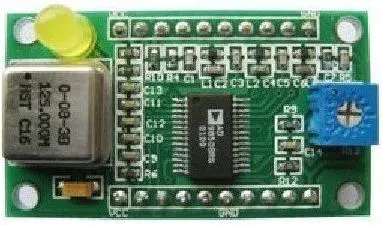
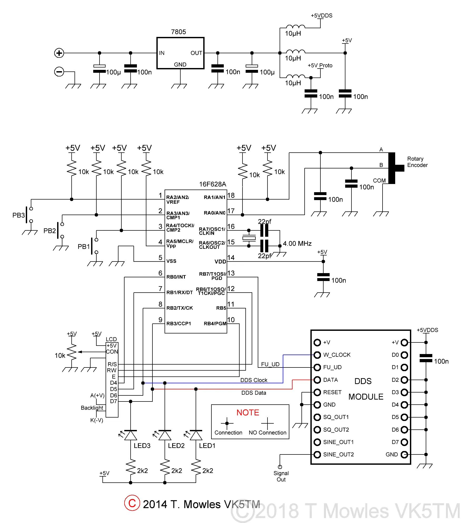
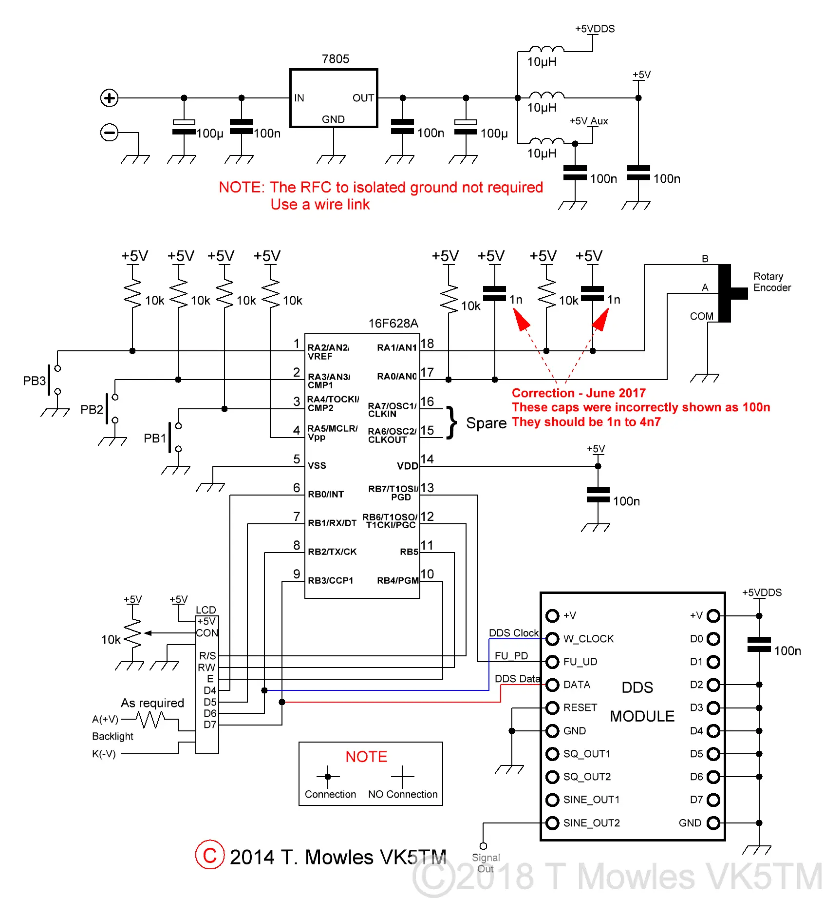
The AD9850 Module uses a 125MHz oscillator module while the AD9851 module uses a 30MHz oscillator. For all intents and purposes, they look identical unless you have a magnifying glass in hand. Because I needed to get this done relatively fast, I again turned to the internet to see what was available. There is quite a bit out there, ranging from ultra simple to top of the line with all the features you'll never use. One site is that of Craig Johnson AA0ZZ, designer of the Pic-El board. The Pic-El board is a teaching system for PIC micro's and among one of it's subjects is a DDS system using the AMQRP's DDS60 daughterboard. Not needing all the various extra's on the Pic-El board, I designed my own with just the bare essentials. My circuit diagram is shown below, along with version 1 of the pcb. I say version 1, because I must have been having a really good day when I designed it, I left some bits out! (Click schematic for larger view. Click again to close.)
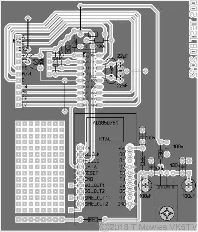
I have redrawn a version 2 of the pcb, but have not as yet made it, so there may still be a mistake or 2 in it, but here is a picture of it for interest.
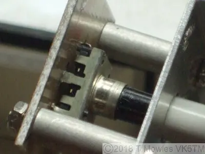
I used the file 'PEGen60c.HEX' from Craig's site to program the PIC with and it actually worked first time. Here are a couple of pictures of the board as it currently is. The LCD is a blue background with white characters type and the encoder (the bit with the big silver knob partially hiding) was a volume control from a stereo system. For mode and up/down buttons, I used 3 buttons from the junk box. They are just a push to make/release to break type.
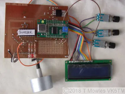
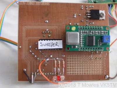
And yes, I was still having a good day (not) when I made this pcb, as I made it back to front. Luckily, some pcb's I was making for somebody else came out correctly. The eagle eyed will notice the label saying "SWEEPER" on the PIC. One of the other things I need is a sweep generator to align my FT-7. Looking around the 'net, there is not much in the way of simple software that will do the job without having to redesign the board or doing a major rewrite of the software. Luckily, while going through the DDS folder on my computer, I found a piece of software that almost fit the bill exactly. It was written by Bob Okas, W3CD,(now SK) to control the DDS30 daughterboard in the Pic-El board, like the previous piece of software. The only thing was, it was written for the AD9850 and I wanted to use the AD9851. A little bit of investigation and time later, the changes were made for the AD9851 and again, it worked first time. There are a couple of things in the software that need pointing out. Firstly, there is mention of a 'beep' when a button is pressed, that is not implemented in the pcb design. Secondly, there is a software routine that uses the three LED's to indicate various things. I did not find it particularly useful (I didn't remove it) and with the values as shown, the LED's are pretty dim. You will need to use low current, high brightness LED's if you want to use them.
Update 17 May 2012
A quick update. I have changed the code to remove the crystal and run the PIC from it's internal clock source in the SweepGen code. This leaves two pins spare and if the MCLR in code is set to internal, that will give one more extra pin. The code version is 1.1e and can be downloaded below. Led code has also been removed from this version. Have also posted a modified version of the PicGen6 asm code and renamed to ver7.0a, but please note, I have not tested it yet. There is also code to use the DDS as a VFO (PEGen2-1f, download below), but be aware that you will probably need extra filtering and to boost the output level. It has dual VFO mode, which can be changed to single VFO (see code comments). There are a few more things on the drawing board which will be written up here as and when I get it finished/working properly. Here is the modified schematic. I have not redrawn the PCB layout, all I did was to remove the crystal and it's two capacitors. Proper pcb layouts etc will be posted when I have finished fiddling with it, but if you want the current one (it's in Sprint Layout format, a free viewer is available), you can contact me via the contact page, through QRZ.COM or I am on several Yahoo/Groups.io groups (BITX20, dds-vfo, FoxTango, GQRP ) as augustinetez (don't ask, Yahoo made it up). (Click picture for larger view. Click again to close.)
Update 16 July 2012
One of the things needed for a signal generator, is to be able to adjust the output level to be a known quantity. A pre-requisite is a signal of known amplitude, to which you can apply known attenuation. Along that vein, I have been playing with controlling the output of the DDS chip itself. The output level of the AD9851 is set by the value of the RSET resistor. On these modules as they ship, that resistor is 3900 Ohms. There is not a great deal of info on the 'net to do a quick and dirty ALC (Automatic Level Control) directly on the chip. However, on the midnight design solutions website, as part of the antenna analyser project, was a couple of ideas, one of which is shown below. (Click picture for larger view. Click again to close.)
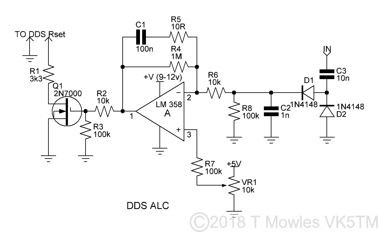
Note that in the original, D1 & D2 were 1N5711 Schottky diodes. The circuit was made up on the prototyping area of the pcb and while it sort of worked, it wasn't really successful. To start with, the control range on the pot was extremely small (anyone with a hand tremor would not have been able to set it at all), and it did not control the level very well over the frequency range. So I tried various ideas using the other half of the LM358, of which all were worse. Leaving it aside for a few days (and doing some paying jobs for a change), I formulated what you see in this next schematic.(Click picture for larger view. Click again to close.)
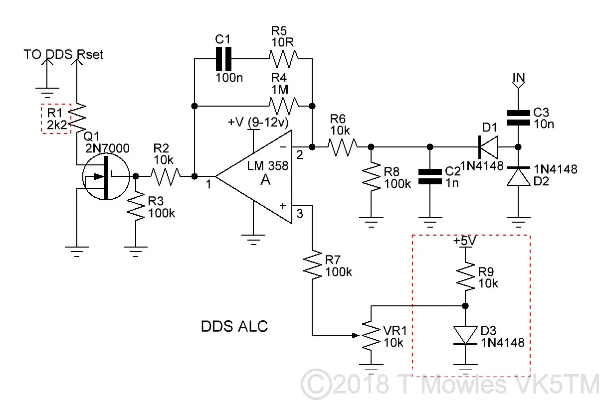
There are two main differences to the first try. Firstly, the reference voltage for the adjustment pot was changed from the full 5v to approx .6v by adding a 10k resistor feeding a 1N4148 diode. It helped, but the adjustment range is still fairly small. Secondly, the 3900 ohm resistor was changed for a 2200 ohm resistor. This had two effects, the adjustment range was better and the output level had increased by about 25%. Sadly, while the level of the output could be maintained over a small range of frequencies, it is still not satisfactory over the whole frequency range. The inbuilt low pass filter of the DDS module is partly to blame here. I need to come up with a different idea, one that actually works, so I'll put on the thinking cap (and hope it doesn't blow off in the wind around here of late), to see what I can come up with.
11 November 2012 - I have had limited succes using the above circuits, so I have abandoned them in favour of a different solution. More info will be posted at a later date.
Update 19 November 2012
Trying to do prototyping with the DDS board as it was with loose wires everywhere was becoming a p* in the a*. So I have made a semi permanent development unit.
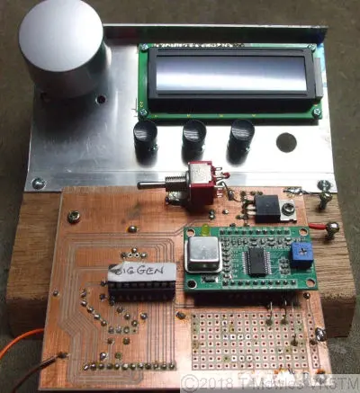
It is made of some scraps floating around the workshop, a piece of aluminium sheet and a leftover bit of skirting board. (For those not sure what "skirting board" is, it's that bit of wood that runs round the wall at floor level). Actually doesn't look too bad, at least the wiring is less likely to keep needing repair. One problem encountered was how to mount the encoder. Rather than waffling on trying to describe it all, here are some pic's of how I did it:-
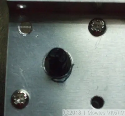
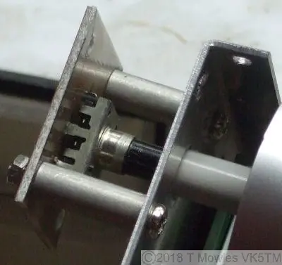
You will notice, right near the bottom spacer, that I bent the rear locating pin out instead of drilling more holes for them (Read - I forgot!).
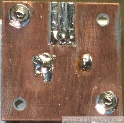
This is just a 35mm square piece of pcb material with the pads scratched out with a sharp knife. I only used two of the mounting holes, it is stable enough not to need all four of them. Here is some preliminary info on the output stage that I am working on. There are two amp circuits I am looking at. One using a BGA2748, which is basiclly just a mmic wideband amp from Philips. They were on special for a few cents each, so I got some to play with. The second circuit uses an LMH6703, which is a current feedback wideband op-amp from National, now part of Texas Instruments. (Click picture for larger view. Click again to close.)
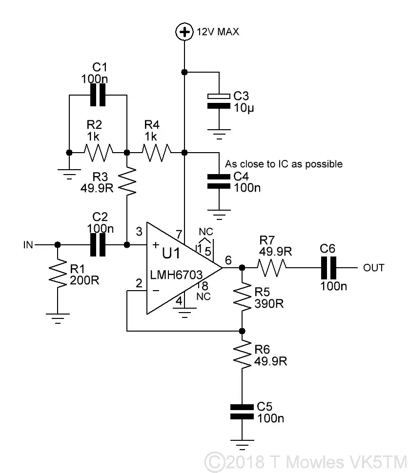
I did not design this, but found it on the website of Gary Johnson, WB9JPS (link at bottom), where he used this for an output stage on a DDS3 unit. It has an output of +13dbm. Gary also wrote a paper analysing the output stage of Craig's (AA0ZZ) DDS unit and offering some alternative thoughts, where the LMH6703 came out as the pick of the bunch. My thinking is to use this, possibly along with the BGA device and a PIN diode attenuator with some control circuitry, to create an ALC unit for the DDS. More to come as I get this prototyped.
Update 25 November 2012
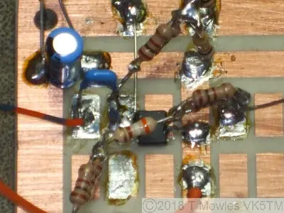
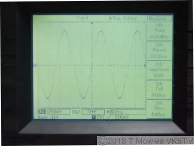
I've built up the output amp on a piece of prototyping board, dead bug style. Despite all the dire warnings in the datasheet for the LMH6703 about pcb layout, it works quite well dead bug style. The IC is in there, right underneath the 390ohm resistor. It is connected to the DDS module directly after the filter and is being run off a 9V supply. With 245.5mV P-P in, it provides 1.25V P-P out into 50ohms.
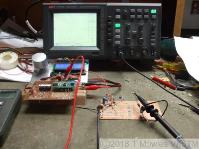
And just to show that this is a "working" workbench, here is a pic of the prototype hooked up in the only piece of clear space on the bench.
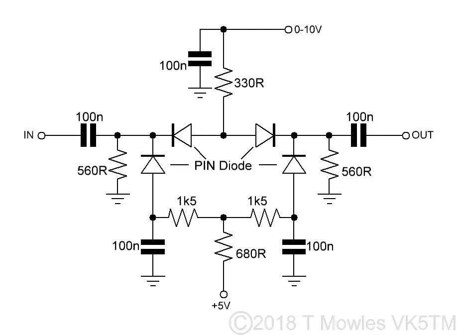
A PIN Diode Attenuator has also been prototyped, but it needs some tweeks to fine tune it. (Click picture for larger view. Click again to close.)
Update 18 January 2013
I've just been out in the workshop (after days of searing heat) and run up a quick output amp using a 2N3904. (Click picture for larger view. Click again to close.)
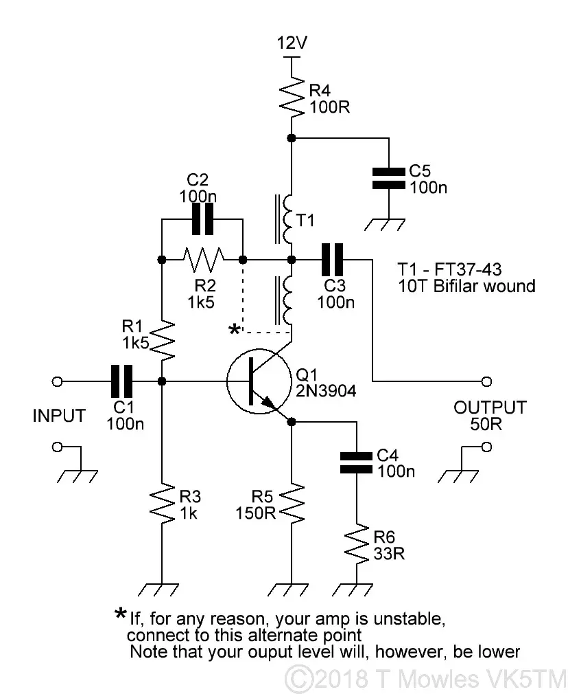
It is a well known feedback style amp. But, just to be different, I have connected the upper part of the biasing/feeedback circuit to the centre tap of the output transformer. It is perfectly legitimate to do so, but note that, depending on your actual components and building style, it may be unstable. If it is, move the connection down to the collector of the 2N3904. The only drawback is that the output level is reduced. In theory, this amp should have an input impedance of 50 Ohms, which is not a good match to the 100 Ohms of the output filter on the DDS module. The result should be a distorted waveform into and out of the amp, but my scope trace showed no problems unless I played with the value of R6. Going too low in value, while increasing the output level slightly, will distort the waveform, indicating a definite mismatch. I have yet to put this amp on the spectrum analyser, but adjustment of the R6 value should get you to a close enough match at the input. This will also shift the output impedance slightly, so, if you need a definite 50R output, add a 6dB 50R attenuator pad. At 12v, the supply current is ~15mA and with my particular AD9851 module, the output level ranges from ~6dBm at the low frequency end to ~8dBm in the middle and ~5dBm at 60MHz (into 50 Ohms). There is a very good site for homebrewers that has much more information on feedbacks amps, measurements and a whole lot more, by Todd, VE7BPO (link below). This is where I got my inspiration to try this out. If you have not seen his site and are a keen homebrewer, I highly reccomend a visit. It has come to my attention that the PEGen60c code (on Craigs website) and PEGen70a.asm below, will only work properly with an optical encoder. I am working on making the ver7 code work with a mechanical encoder.(Done 14/01/13)
Update 6 February 2013
I have restarted work on an ALC (Automatic Level Control) circuit again and will post that information when I get it finalised. The main idea of this is to maintain a constant output level over the entire frequency range of the module. For signal generator mode, that would be 0dbm while +7dbm seems to be the average needed for VFO mode. In the meantime, I have measured the output of the DDS, using the spectrum analyser and the LMH6703 output stage. The level ranges from +8dbm at 1MHz to +10dbm at 5MHz, down to +7dbm at 30MHz. By 60MHz, it has dropped to -1dbm. The figures for the 2N3904 stage will be added later. I have also drawn up what, for me, will be the final pcb of the DDS controller. The amp/buffer stages and ALC will be on a seperate pcb, this way, if you have a favourite output stage, you can use it with the controller as it stands. For those working in Imperial measurements, 81.5mm = 3.25 inches and 91.4mm = 3.6 inches. For those that may wish to make their own copy of the pcb, the file is in the Downloads section below. Please see the Homebrew Menu page for details of a free viewer that you can download and use to view and print the file. (Click picture for larger view. Click again to close.)
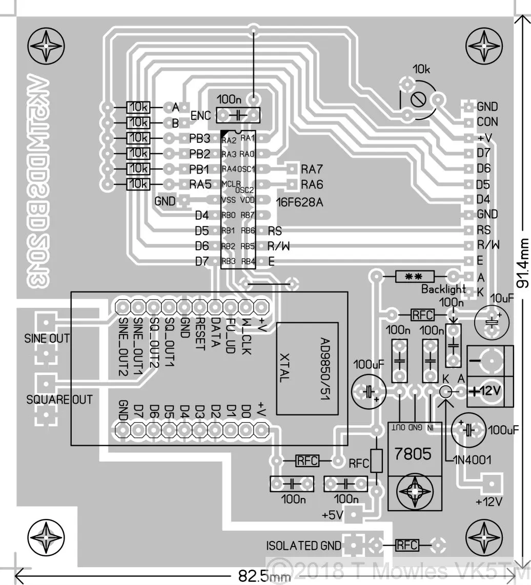
A note on the items marked as RFC. On my current pcb, I have used 10uH chokes, the ones that look like resistors. You can use any style of choke you like, providing that it can handle the current. The value of the RFC connected to the 'ISOLATED GROUND' may need to be a higher value than 10uH, you can experiment for the best result. The component marked '**' and connected to the A terminal for the LCD backlight may or may not be needed depending on your particular display. Some display backlights operate from lower voltages than 5V, check the data for your display and calculate the value of resistor needed if necessary, otherwise place a wire link there. Also, mount the resistor (if used), above the pcb by a couple of mm to allow air to flow round it.
19 July 2014
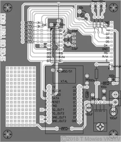
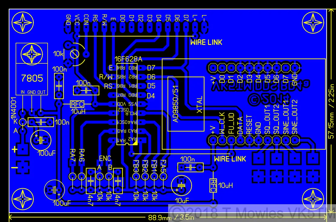
After several builders requests, here is a more compact version of the DDS pcb (V4a, available to download below).((Click picture for larger view. Click again to close.)
Downloads
These files are provided free for personal use ONLY. I retain all copyright on all works published on this website. They may NOT be used in any commercial or profit making enterprise of any kind without the express WRITTEN permission of the copyright holder.
I am aware of at least one outfit making copies of my pcb's without even the decency of asking permission!!!!
(Right click and 'Save as..' or what ever is required by your browser) 1st April 2013 - The code files have been updated to send a zero frequency initialisation at the beginning of start-up as per the datasheet. 18th Jan 2014 - While some of these files have been marked as "for mechanical encoder only", some builders have reported that they do in fact work with optical encoders. Guide for using the Sweepgen software. SweepGen_1-1a_release_notes.txt SweepGen_1-1a.asm AD9851 hex file: SweepGen_1_1a.hex AD9850 hex file: SweepGen_1_1a_AD9850.hex SweepGen_1-1e.asm AD9851 hex file: SweepGen_1_1e.hex AD9850 hex file: SweepGen_1_1e_AD9850.hex PEGen2-1f.asm AD9851 hex file: PEGen2_1f.hex AD9850 hex file: PEGen2_1f_ AD9850.hex PEGen70a.asm - for optical encoder only AD9851 hex file: PEGen70a.hex AD9850 hex file: PEGen70a_AD9850.hex PEGen7_1a.asm - for mechanical encoder only AD9851 hex file: PEGen7_1a.hex AD9850 hex file: PEGen7_1a_AD9850.hex The following code has major changes as regards the function of the buttons and the addition of an extra button. It is also coded for mechanical encoders only. All other functionality is the same as previous version 7 software. See the top section of the ASM file for the changes. PEGen7_2a.asm - for mechanical encoder only AD9851 hex file: PEGen7_2a.hex AD9850 hex file: PEGen7_2a_AD9850.hex PEGen7_4a.asm - for mechanical encoder only. Auto save frequency and 100kHz step added. Extra button removed. See head of asm file for details. AD9851 hex file: PEGen7_4a.hex AD9850 hex file: PEGen7_4a_AD9850.hex The following code has these functions:- IF offset Band limits to prevent out of band Transmitting. Save last used frequency automatically. Dual VFO. See the top section of the ASM file for the instructions on setting your preferences. Updated 18 Jan 2014 to include AD9850/AD9851 selection at top of file. PICELGen2_4a_offset.asm There is no hex file posted as you will need to modify the options to suit your use. The following version is a requested mod from a ham in DK. It is for use as a TX VFO and will only output a signal when PORTA,5 is pulled low. Also, the frequency cannot be changed when in TX mode. 60m band has also been added. PICGen23c_PTT.asm There is no hex file posted as you will need to modify the options to suit your use. DDS Controller PCB File is in Sprint-Layout 6 format. See PCB Info page for details. DDS Controller PCB V4a File is in Sprint-Layout 6 format. See the PCB Info page for details.
References & Links
All off-site websites open in a new page.
Craig's website. Scroll down for the Pic-El code
The website of Gary Johnson, WB9JPS. The LMH6703 is on his electronics page.
The website of Todd, VE7BPO.
