News, Updates and Other Minutiae
August 2025 UR5WHK has created another version of the AD9833 project with a 128 X 32 OLED display. You can find it under the Gallery menu - it is on the same page as the MAX7219 version.
July 2025 UR5WHK has created an updated version of the AD9833 project which now includes a MAX7219 based LED display. Code updated 10 July 2025. Code updated again 15 July 2025. You can find it under the Gallery menu.
March 2025 In something of a "Seniors Moment", I forgot to update the homebrew menu and this section relating to a project I did late 2024. That project is an update of one from the RSGB Radcom magazine of Sept 1999 - 'Turn Your Dip Meter into a Signal Generator'. Presented here as 'Grid Dip Meter (GDO) Add on' under the Homebrew menu.
November 2024 Phillipe F6ETI has done some serious testing on the Noise Canceller and shown it works up to 72MHz and is usable with some loss at 145MHz. Links to his website with photo's, video's and description of the testing on the Noise Canceller page.
Privacy Policy uploaded. GPDR and all that stuff In accordance with various bits of legislation around the world, either currently in force, about to come into force or proposed, you will now find that annoying "We use cookies" notice at the top of this website. The full Privacy Policy is available at the Privacy Policy link in the footer at the bottom of the page. (If you don't know what GPDR is, Google it. Real scary shit for ANYBODY with a web presence.)
Add Auto Filter Switching to the DDS Signal Generator
Would you like to add Auto Filter switching to your DDS project? Here's how.
I have been asked to make many customised mods to the DDS software during the past year, mostly minor and I didn't feel it worth putting up on the website. However, one mod that is worthwhile, is to add Automatic Band Filter Switching. I won't redo the software as listed on the DDS page, as it is quite easy to do, so read on. Firstly, for the Version 7 software: The first thing that needs to be done are some minor hardware modifications, shown here in RED.
Click schematic for larger version. Click again to close.
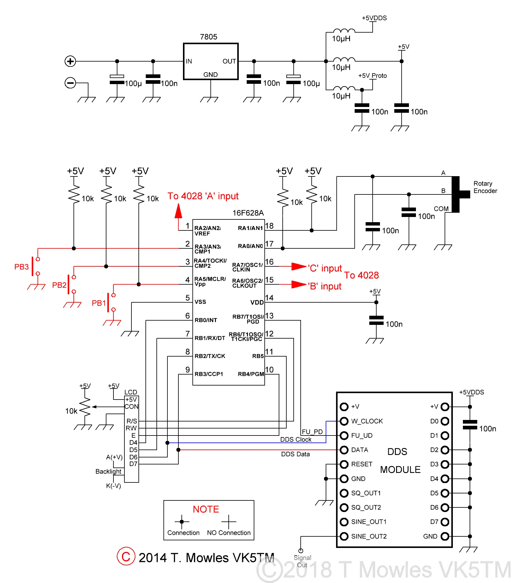
The reason for moving the switches to (in particular) pin 3 (RA4) and pin 4 (MCLR) are: RA4 (pin 3) is an open collector output when configured as an output pin, requiring a pull-up resistor and inverted code logic to make it switch. Much easier on the brain cells to make it an input. Pin 4(MCLR) is an input only pin and we need output pins for this mod. Before adding the band switching code, we need to make some changes so that the PIC recognises, firstly, that the switches have been moved to other pins and secondly, that we need the various pins to be either inputs or outputs. This is a three step process: First, the config word at line 196, there may be slight variations in line numbering depending on what mods you may have already done or which version of the software you are modifying):

Must be changed to:

This allows us to use the MCLR pin as an input pin. Second we need to change the assignments of PB_1, PB_2 and PB_3 (if used). In the version 7_4a code at lines 410 & 411, PB_1 and PB_2 have been equated to the numbers 4 & 3 So, PB_1 becomes pb_1 equ 5, PB_2 becomes pb_2 equ 4 (and PB_3 becomes pb_3 equ 3 if used in the version you are modifying). This is a screenshot of the version 7_4a code, showing where to make the changes.
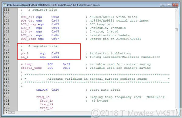
Thirdly, we need to set the appropriate pins of PORTA to inputs and outputs. Below is the original 7_4a code.
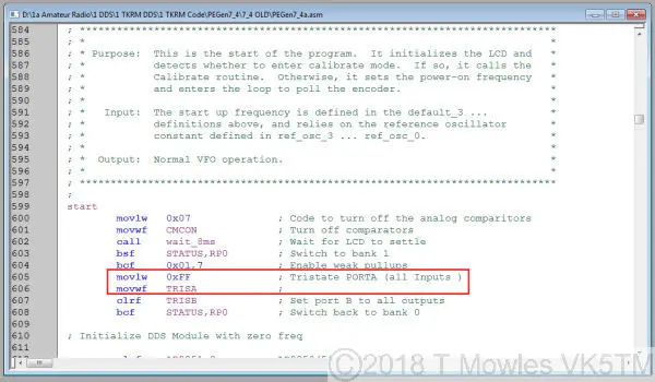
So we need RA 0, 1, 3, 4 & 5 to be inputs and RA 2, 6 & 7 to be outputs. I find it much easier to use binary to do this (using HEX really confuses this old brain) as it is easier to remember 0 = output and 1 = input so the code becomes: (RA 7 6 5 4 3 2 1 0) movlw b'0 0 1 1 1 0 1 1' (don't put spaces between numbers, it is here to show the correlation to the PORTA line above) movwf TRISA At this point, after making the code modifications, program the PIC, put the PIC back in circuit and check that everything still operates as it did before. If all is OK, move on to the next step of the procedure - adding the filter switching code. You need to modify the 'show_freq' routine:
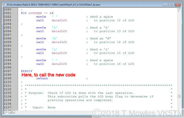
What to put: I have been very original and called the new bit of code 'filter', so you need to insert: call filter between the '#ENDIF' and 'return' (don't forget to remove that pesky ; if it's still there) or the very last 'return' in the same routine in other versions. At the very end of the asm files are the delay routines, so I would normally put this new routine immediately above it. Ignore the line numbers on the left of the following picture, it is from a different, highly modified file, (this is just the start of the new routine).
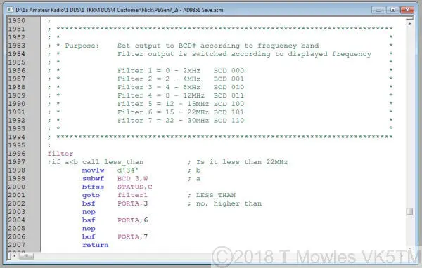
The complete new piece of asm code is available to download below.
Code explanation
Ok, firstly, I have taken the lazy way out to implement the band switching. Why make things any more complicated than they need to be, hihi. I have taken the 0 - 30MHz range and split it into the following 7 segments: 0 - 2MHz (actually 0 - 1,999,999 Hz) 2 - 4MHz (again, actually 2,000,000Hz to 3,999,999Hz) 4 - 8MHz (actually - well you get the idea) 8 - 12MHz 12 - 15MHz 15 - 22MHz 22 - 30MHz For those working the low bands, more info at the end, under Customising. The next thing I have done, is to make the switching activate according to the frequency displayed on the LCD. In the DDS code, to display the frequency on the LCD, the code takes the 32bit value of freq 0...3 and converts it into packed BCD format. The packed BCD format uses 4 bits of each 8 bit word to represent a number from 0 - 9, so you can store 2 numbers in each 8 bit word. There is a bit of jiggery pokery involved to get the aforementioned BCD digits onto the LCD, but we do not need to concern ourselves with that here. What we do need to know is when the MHz digits change and what they are. These MHz digits are contained in the file BCD_3 (remember, I took the lazy way out, so BCD_2...0 can be ignored). Example: If the LCD is showing 10, something MHZ, the BCD_3 file (in binary) will look like this: 0001 0000 > the first 4 bits equal decimal 1 and the second 4 bits equal 0 = 10 on the display. Again, assume the LCD is showing 22 something MHZ, the BCD_3 file will look like: 0010 0010 > the first 4 bits equal decimal 2 same as the second 4 bits = 22. EACH 4 BITS of BCD_3 represent a single number and both of them relate to the xx,000,000 part of the frequency. So, to work out where we are in the frequency range, we need to compare BCD_3 with a 'number'. If BCD_3 is lower than 'number', we can do thing 1, if it is equal or higher, we can do thing 2. Firstly, we need to find what 'number' will be for the comparison (and for those that have looked at the code and gone, how does d'34' = 22MHz?), this is how it is done. Using the calculator set to programmer mode in Windows helps here. As shown above, BCD_3 will look like 0010 0010 for 22. To get 'number', you need to convert ALL 8 bits of BCD_3 to decimal (just as you would if it was an ordinary 8-bit file). So 00100010 = 34 in decimal. That's how 22MHz becomes d'34' using just BCD_3. Here are the other segments:
(Click table for larger version. Click again to close.)
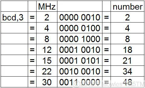
Hopefully, that was a bit clearer than mud and you can now work out what the code does. Hang on, why do we start testing at 22MHz and not 30MHz? And why from the highest frequency down? The answer to the first question is logic and it depends on how you have split the range 0 - 30MHz up. In this case, the highest segment is 22 - 30MHz, so if BCD_3 is not lower than 22MHz, we must be in the 22 - 30MHz segment. As for the second question, it is only one way of doing it and I picked the LESS THAN way. You can work the other way round, from lowest to highest frequency, but you need to use a different comparison technique.
The decoder bit
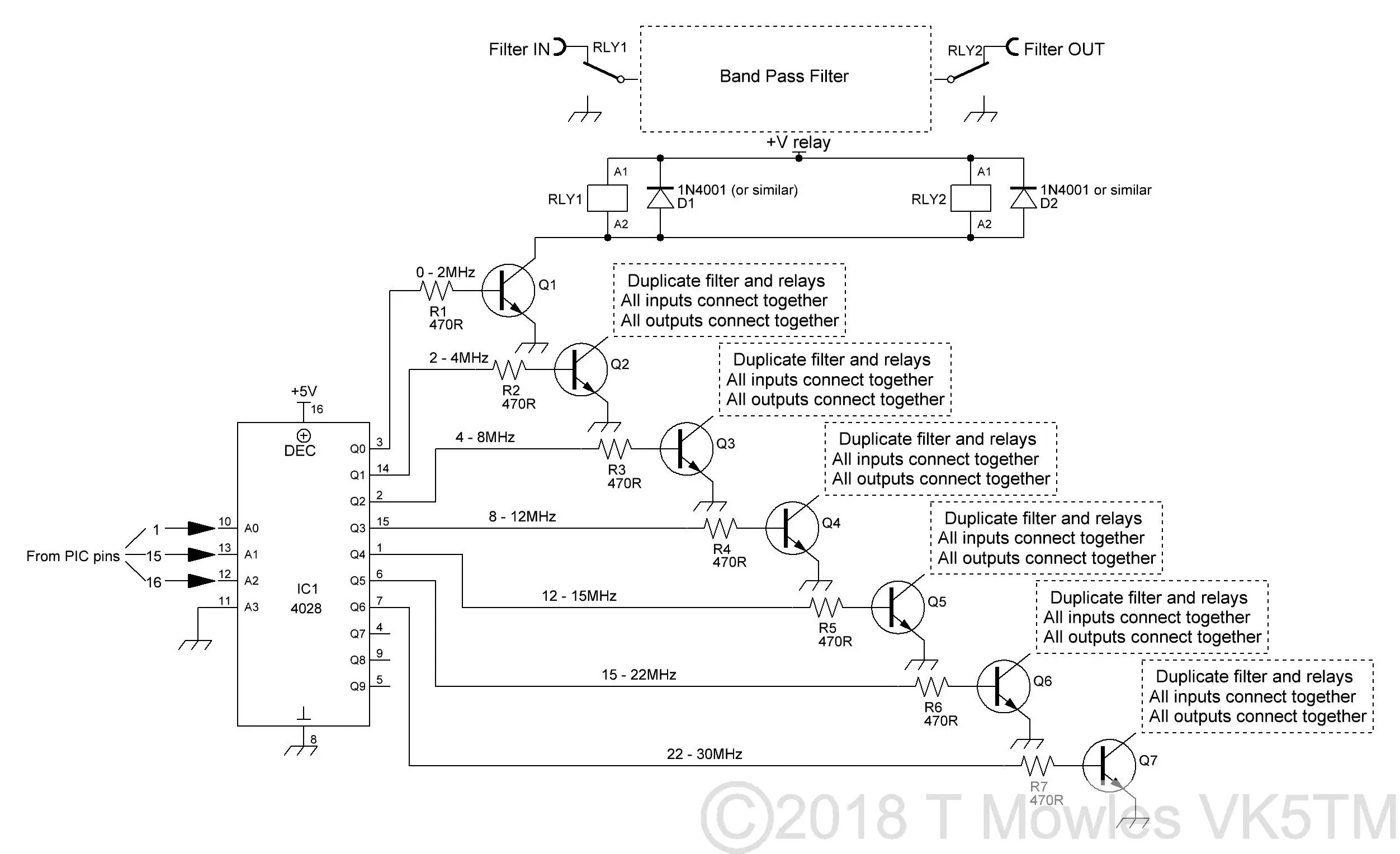
Below is a schematic of a 4028 based decoder for switching seven filters. You can use whatever is available that will switch in accordance with the BCD code output by the PIC or even modify the code to suit what you have. I won't make any comments on construction of the decoder, as everybody has their own favourite way of doing things. Likewise, the filter topology is up to you. There is still another BCD code available with three control lines that will enable switching of an eighth filter or you can get up to ten with the 4028 if you have a spare pin on the PIC available and modify the code accordingly.
Click schematic for larger version. Click again to close.
Customising it
As mentioned above, the code is setup to switch seven filters, with one more BCD code available to add an eighth filter. Utilising a spare pin on the PIC will allow for up to ten filters. I will leave how to code that up to you. You might, for instance, use the extra filter for 6m. As mentioned early on, for those of you working Low Band, it is possible to change the code to work down lower. You will need, however, to include some comparison testing on the BCD_2 file as well as the BCD_3 file. One other thing you might want to consider is re-arranging the BCD sequence in code so that the 4028 switches pins in sequence ie pin1,2,3,6,7,14 & 15, rather than following it's logical outputs (Q0, Q1 etc). It would make laying out a pcb or even just wiring dead-bug style somewhat simpler. As another exercise, you might also have a go a writing some code for another PIC to act as the decoder.
Modifying the version 2_4a software
Firstly, the hardware mods are the same as above, as is the config setting. Next is the change to the PortA pin directions:

Needs to be changed to: PORTA_CONTROL equ 0x3b ; b'00111011' Port A 0,1,3,4&5 inputs, 2,6&7 outputs Note that the IFDEF DUAL_VFO, ELSE & next PORTA_CONTROL equ and ENDIF statements have been removed. The value has been input as a HEX value by virtue of how the program has been written.

The next step is to redefine the push-buttons:

Becomes: ; ; A register bits: ; PB_3 equ 0x03 ; PB also on this pin PB_2 equ 0x04 ; Bandswitch Pushbutton, PB_1 equ 0x05 ; Tuning-increment/Calibrate Pushbutton The SPEAKER equ at line 755 is removed as it has no relevance here.

You will also need to remove these lines, they are not replaced with anything:

To install the filter switching software, add this at line 3314 (it is in the show_freq routine immediately before the final 'RETURN': call filter You can then add the Auto Filter Switching routine (contained in the file filter.asm) at around line 3831, which is immediately before the delay routines. There is no particular reason to put the routine in this location, it is just that I prefer the delay routines to be the last piece of code, making it easier to find if I need to change them. As before, the filter switching will change according to the displayed frequency, regardless of any offsets applied. Please note that you are limited to a maximum of 8 filter ranges because this software uses all 3 push-buttons As always, I am happy to help if you are really, truly, absolutely stuck with implementing these changes. But, I will request a donation (how much is up to you) to help with the cost of running this site.
Downloads
A builder has found an error in the code which has now been corrected. Apologies to those that may have experienced problems. These files are provided free for personal use ONLY. I retain all copyright on all works published on this website. They may NOT be used in any commercial or profit making enterprise of any kind without the express WRITTEN permission of the copyright holder.
(Right click and 'Save as..' or what ever is required by your browser) filter.asm
