News, Updates and Other Minutiae
August 2025 UR5WHK has created another version of the AD9833 project with a 128 X 32 OLED display. You can find it under the Gallery menu - it is on the same page as the MAX7219 version.
July 2025 UR5WHK has created an updated version of the AD9833 project which now includes a MAX7219 based LED display. Code updated 10 July 2025. Code updated again 15 July 2025. You can find it under the Gallery menu.
March 2025 In something of a "Seniors Moment", I forgot to update the homebrew menu and this section relating to a project I did late 2024. That project is an update of one from the RSGB Radcom magazine of Sept 1999 - 'Turn Your Dip Meter into a Signal Generator'. Presented here as 'Grid Dip Meter (GDO) Add on' under the Homebrew menu.
November 2024 Phillipe F6ETI has done some serious testing on the Noise Canceller and shown it works up to 72MHz and is usable with some loss at 145MHz. Links to his website with photo's, video's and description of the testing on the Noise Canceller page.
Privacy Policy uploaded. GPDR and all that stuff In accordance with various bits of legislation around the world, either currently in force, about to come into force or proposed, you will now find that annoying "We use cookies" notice at the top of this website. The full Privacy Policy is available at the Privacy Policy link in the footer at the bottom of the page. (If you don't know what GPDR is, Google it. Real scary shit for ANYBODY with a web presence.)
Grid Dip Meter (GDO) Add on
An add on for a GDO to level the signal amplitude.
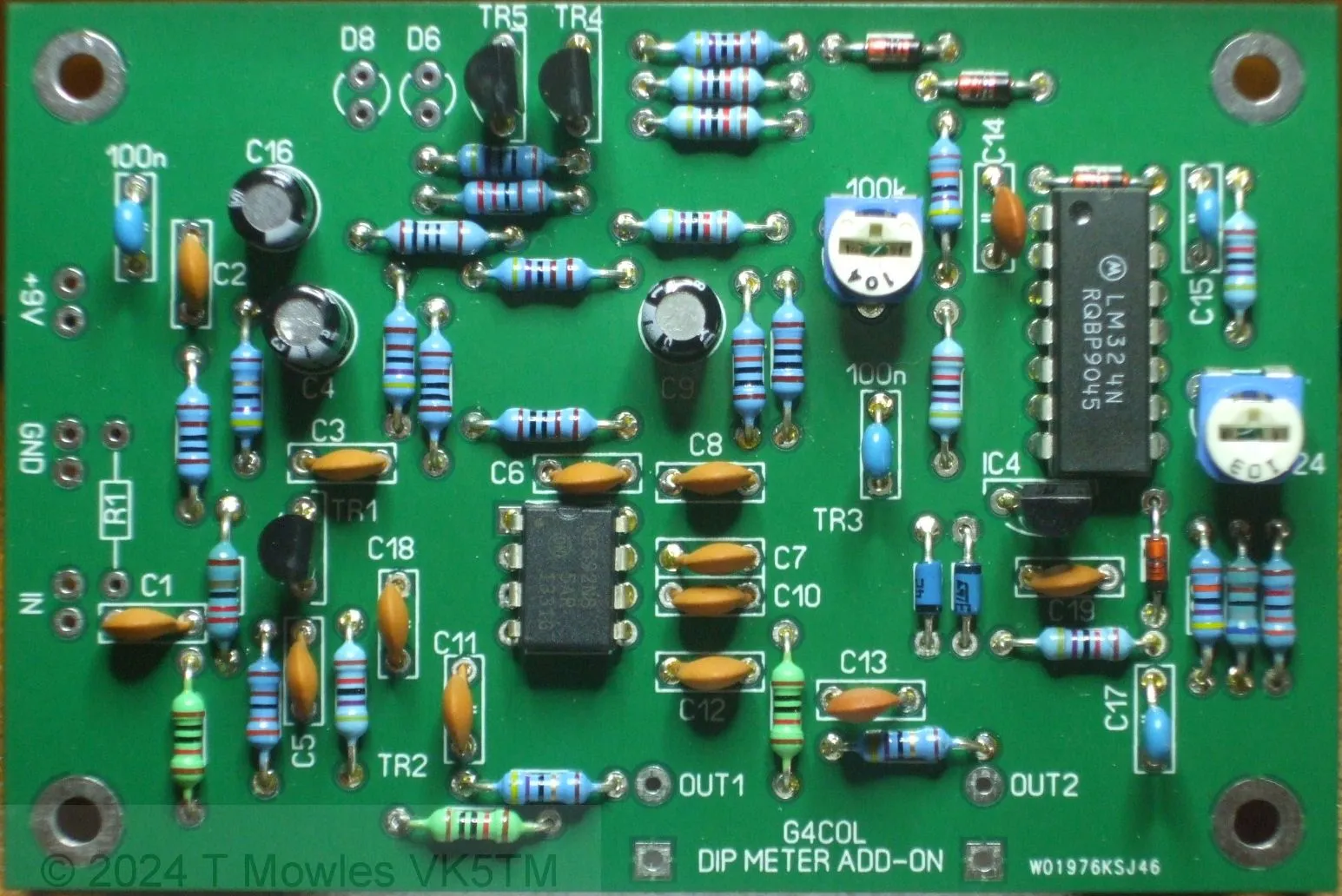
Firstly, I would like to point out this is not one of my designs, but a project of Ian, G4COL, that was originally published in the RSGB magazine Radcom in September of 1999. Ian was most helpful in sorting some errors that showed up in the original article and he has most graciously granted me permission to present my tweaked version here on my website. The What and Why. Firstly, the what: This project is a levelling amplifier add-on for a GDO so it can be used as a signal generator with a constant level output signal (but not confined to that use). Why: I was working on another project that was showing some odd behaviour when driven by my AD9850 based sig-gen and being suspicious it might be related to that sig-gen, I figured trying an old style analogue sig-gen would be a wise move to check on what was going on (think various spurii and harmonics). Only problem is, my only available analogue sig-gen doesn't go below 10MHz (I needed a 1.8MHz signal) and I really didn't feel like building something, so I looked to buy a cheapy sig-gen and found a GDO at a very good price. I was going to modify the GDO with a buffer and output socket to pick off it's signal, but when it arrived, it was in such pristine condition that it would have been sacrilege to mess with it. Oh, it wasn't the AD9850 sig-gen causing the odd behaviour by the way, another story for another day, maybe. The Project Ok, lets get in to this project with the schematic, the parts in red are my tweaks .
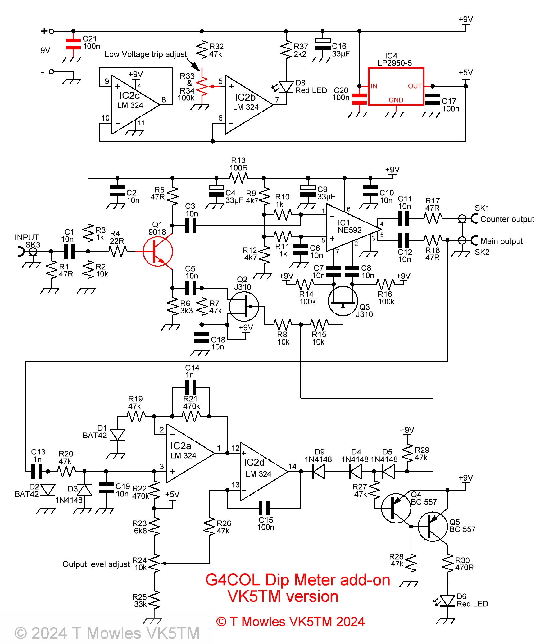
Schematic description. I won't go in to a component by component description, for that I refer you to the original article - you can buy an archive DVD from the RSGB for a reasonable price if you don't have access to the relevant issue of Radcom (I will ask the RSGB for permission to make the original article available here - Update 20 March 2025 - I did ask, via email, and as per usual got no response). The component numbering is mostly as per the original but note that there are some discontinuities as was published in the original article. There are also other errors in the original article:- reference is made to IC2b as part of the detector circuit, that should be IC2d. R14 should be 100k not 10k. D1,2,4 & 9 are shown the wrong way round on the pcb overlay in the original article and should be reversed. Starting from the top of the schematic and working left to right: This is (obviously) the power supply section - the project was initially designed to be run off a 9V rechargeable battery (there is a recharge circuit - not utilised here - in the original article) - please don't be tempted to run the project off 12V, the Magic Smoke may eminate from something it shouldn't 🥴. IC2c is the unused section of the LM324 and is setup as per recommendations for unused sections of op-amp ic's. Following that is IC2b and is the low battery voltage indication - adjust the trimpot labelled as R33 & 34 so that the LED comes on at ~7.8V if running this on a 9V battery. R33 & R34 in the original was two seperate resistors as part of the voltage divider for the low battery set, as you can see, I have replaced them with a trimpot. In hindsight, R32 probably could have been left out and the trimpot connected directy to the 9V line, a 10-turn trimpot should be used if you go that way. Last in the line is the 5V regulator that is used as the reference for the detector circuit. Originally a 78L05 was used but that will get a bit iffy at low battery voltages so I replaced it with a low drop out regulator. On to the middle section of the schematic. This is a variable gain amplifier utilising the NE592 video amplifier ic and a couple of J310 FETs (at the time this webpage was published, August 2024, NE592's are still available but only in smd format. I was lucky enough to find a supplier with some of the DIP version still available). The original used a 2N2369 fast switching transistor as the input buffer, but they are getting thin on the ground so I substituted a 9018 which works perfectly well in this application. Other than the J310's, there is nothing particularly special about any of this section. Also, the original had a pickup loop etched in to the pcb and the GDO coil was inserted or positioned close to this for input to the unit. As you will see from the assembled pcb below, I have changed that to just input pads to make my version a bit more versatile. Levelling is performed by detecting the output level from the NE592 via the bottom section of the schematic utilising 2 sections of the LM324 (IC2a & d) and applying a correction voltage to the two J310's. Two J310's, one in the input buffer and the other on the NE592 were used to obtain a higher gain attenuation level. The output level will be approximately -10dBm in to a 50Ω load and can be adjusted with R24. Q4 & 5 are used to light an LED to indicate when the input level is too low and levelling is lost. Note that as it currently stands, the input level to this circuit should be limited to 40-50mV - I have more to do in adapting this to my DDS unit to allow higher input levels.
This is a page in progress with more to come as and when I can get to it.
